

Exhibitor information
ASMADE Semiconductor Technology Limited
深圳市卓兴半导体科技有限公司
深圳市卓兴半导体科技有限公司
ASMADE TECHNOLOGY LIMITED, a national high-tech enterprise and Chinese SRDI (Specialized, Refinement, Differential, Innovation) "Little Giant" Enterprise, founded by an international leading motion control expert team. Gathering the industry's top packaging technology experts, ASMADE focuses on the research, development, and manufacturing of high-precision semiconductor equipment, as well as sales.
The main machines include Semiconductor High Precision Packaging Equipment, Power Device Packaging Solution, Mini/Micro LED Packaging Solution, intelligent control equipment, and a semiconductor packaging process management system. Dedicated to providing one-stop semiconductor packaging process die bond solutions. The machines have independent intellectual property rights.
Booth No.:
E5.5272
Country:
Product Category:
Surface mount technology
SiP
Components manufacturing
Application Area:
Industrial Electronics
Communication Systems
New Energy
Aviation&Space Technology
Military Electronics
Product material
Conventional Products
Product Category:
Surface mount technology
Application Area:
Exhibitor news
News Title
News Contents
Publish Time
Semiconductor Silver Epoxy Die Attach Machine | Integrated Dispensing + Mounting Process, New Equipment for Multiple Applications
March 19, 2026
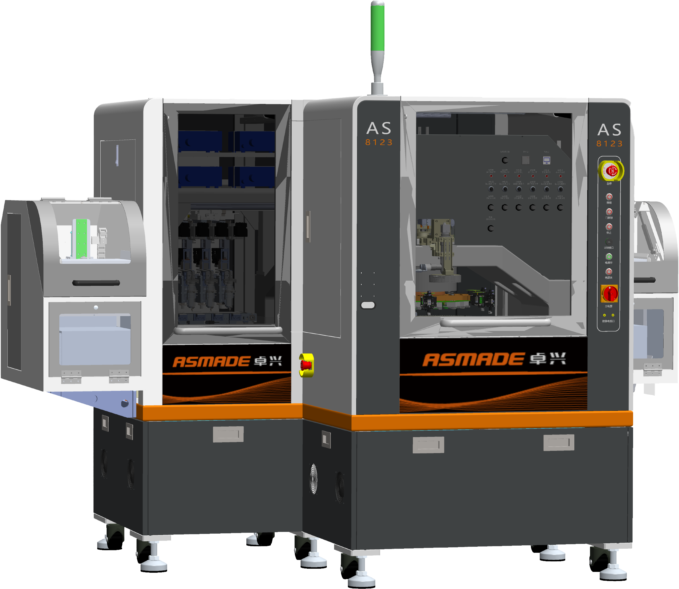
A 2-in-1 semiconductor dispensing and die bonding equipment for silver paste and other adhesives, supporting dot dispensing, pattern dispensing, and dip coating processes. Applicable to small-signal silver epoxy process power devices, sensors, SIP, Chiplet, IC, MOS, and other products.New Equipment Solution: Turret-Type MountingThe turret-type mounting mechanism is an innovative chip mounting method pioneered by Zhuoxing Semiconductor in the industry. The semiconductor silver epoxy die attach machine is equipped with six individual nozzles and adopts a multi-process parallel operation design. It performs chip mounting through multi-station rotating cycles, enabling simultaneous pick-up, mounting, and real-time vision compensation. This achieves the dual effect of "non-stop mounting" and "shortened production cycle," increasing production efficiency by 60%.The standard configuration of its mounting worktable is as follows: Meanwhile, Zhuoxing Semiconductor's self-developed pressure control system adopts direct motor connection, enabling the mounting structure to maintain stable pressure control under different resistances and achieve dynamic pressure control. Its equipment pressure value: 30-300g (±5g).Adapting to Multiple Processes: Three Dispensing Groups or Optional Dip CoatingThe semiconductor silver epoxy die attach machine supports configuration with up to four dispensing mechanisms. The machine supports both chip dispensing and packaging operations simultaneously, achieving multiple functions with one device. Customers do not need to purchase additional dispensers, providing manufacturers with a better solution.In addition, the silver epoxy die attach machine is suitable not only for dot and pattern dispensing processes but also for multi-needle dip coating processes. Process structures can be changed at any time, truly realizing "one machine, multiple uses"!Dispensing Features:① Compatible with different dispensing controllers to meet customers' multiple process requirements② Optional auxiliary functions such as frame heating based on customized process characteristics③ Enables visual recognition of dispensing positions and supports import of preset patterns and path dispensingDispensing Mechanism:Adapting to Multiple Material Types: Multi-Size Wafers and Custom TraysThe semiconductor silver epoxy die attach machine supports various sizes of blue film feeding, including 2/4/6/8/12-inch wafers, with automatic film expansion for 12-inch wafers. It supports single 6-inch mother-daughter rings, Waffle Pack, and GelPAK, and tray customization is available based on specific requirements.High Precision Guarantee: Downward Vision Accuracy CompensationIn terms of accuracy, the machine's mounting X/Y precision reaches ±15μm, angular error ≤ ±1°, production cycle 22.5k/h. Due to the turret structure design for mounting, Zhuoxing Semiconductor flexibly installs downward vision cameras or transfer stages at stations during actual operation, achieving simultaneous chip mounting and accuracy compensation, with AI automatic accuracy compensation and pressure correction functions.Against the backdrop of increasingly fierce industry competition, Zhuoxing Semiconductor is committed to providing more manufacturers with efficient and precise solutions, supporting the development of the semiconductor industry with excellent packaging technology.About UsFounded by an internationally leading team of motion control experts and bringing together the industry's top packaging technology specialists, we are a national high-tech enterprise and a specialized and sophisticated "Little Giant" enterprise with over 20 years of technological accumulation and market practice, focusing on the R&D, manufacturing, and sales of high-precision semiconductor equipment.Our main products include semiconductor packaging equipment, power device packaging equipment, Mini LED chip transfer equipment, intelligent control equipment, and semiconductor packaging process management systems.We are committed to providing customers with one-stop overall solutions for semiconductor packaging processes. Our products feature fully independent intellectual property rights, and many of our equipment models are industry firsts.
March 19, 2026
Learn More
Multi-Process vs. Precision vs. Speed: How to Simultaneously Balance the Equipment "Iron Triangle" to Improve Semiconductor Packaging Production Efficiency?
March 19, 2026
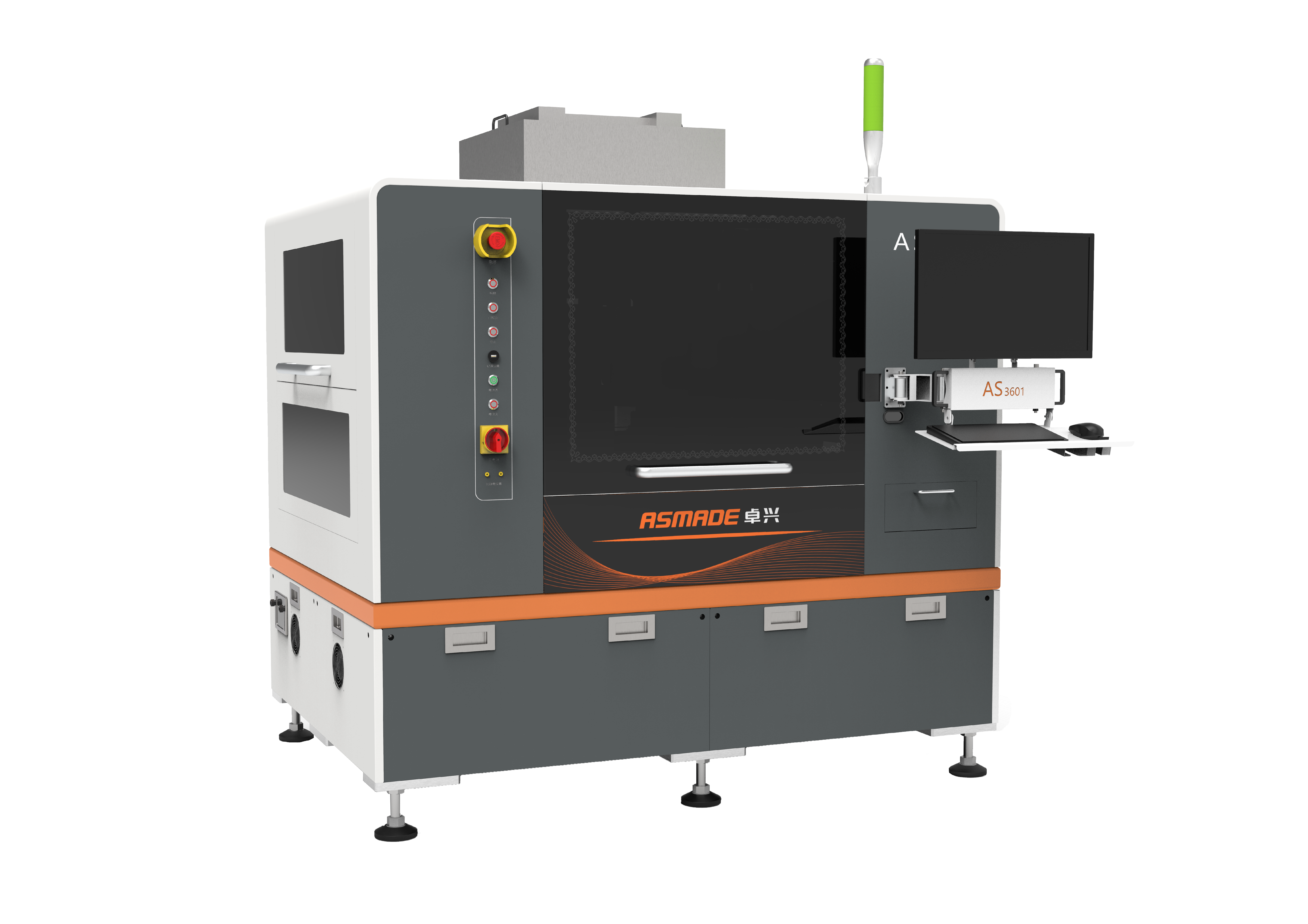
The current semiconductor packaging environment is facing a significant contradiction: the growing demand for complex products versus rigid traditional manufacturing capabilities. Specifically, this contradiction is mainly reflected in two aspects: the multi-process nature of semiconductor packaging, and the current mainstream semiconductor mounting structures. Diverse Semiconductor Packaging Process Requirements:The Prevalence of "One Machine, One Process" Increases Corporate Capital BurdenThe back-end processes of semiconductor packaging involve various substrate materials (lead frames, PCBs, ceramics, glass, etc.) and complex interconnection processes (die attach, bonding, etc.). Different materials and processes have vastly different requirements for equipment, leading to the widespread phenomenon of "dedicated machines for dedicated uses." Lead Frame PackagingCommon processes for lead frame packaging include silver epoxy pasting and eutectic bonding. It faces the pain point of cumbersome line changeovers: a single production line needs to switch between producing silver epoxy pasting products and eutectic bonding products at any time. These two processes require completely different equipment (eutectic bonding requires a heating stage, vacuum adsorption, and high-temperature nozzles). Switching processes means replacing the entire machine, re-debugging, and recalibrating, which can take hours or even longer. PCB Substrate PackagingCommon processes for PCB substrate packaging include silver epoxy pasting and multi-chip integration, where "multi-chip integration" is the biggest challenge. A complex chip (such as SiP system-in-package) may simultaneously contain logic chips, memory chips, RF chips, etc. These chips may come from different wafers, have different thicknesses, different sizes, and even require different pasting processes. How to handle these diverse material inputs is a critical issue. Ceramic Substrate PackagingIn the production of aerospace and military products, many different processes are required, such as silver epoxy, eutectic, ultrasonic, and bonding.It not only faces the challenge of process diversification, but bonding also requires prolonged high temperature and high pressure, posing significant challenges to equipment thermal management, material thermal expansion control, and precision force control.Facing diversified substrates and processes, for many packaging manufacturers, "dedicated machines for dedicated uses" is the current "first solution," but it is not the "optimal solution." It causes huge capital waste, cannot adapt to the normalcy of order fluctuations and process iterations, and its rigid production lines force companies to invest in additional specialized equipment for each new product or process. Therefore, how to break free from the dilemma of repeated investment has become a core issue related to corporate competitiveness. Problems with Mainstream Mounting Structures:Inability to Simultaneously Balance Three Major Demands, Affecting Production CapacityBesides the "dedicated machine" phenomenon, the second major aspect of the contradiction in semiconductor packaging lies in the structure. There is a term in economics called the "impossible triangle," which also applies to semiconductor packaging. The impossible triangle in semiconductor packaging usually refers to the imbalance among "precision," "speed," and "process adaptability." How to solve this "impossible triangle" and turn it into a "process iron triangle" is a question every professional in the packaging industry needs to consider. Efficiency vs. PrecisionAchieving high efficiency requires significant acceleration of moving parts, but this generates enormous inertial forces, leading to unavoidable elastic deformation and vibration in the mechanical structure. If the excitation frequency generated by the motion happens to match a certain natural frequency of the equipment's mechanical structure, it can cause intense resonance, affecting precision.Therefore, Zhuoxing Semiconductor's motion control team designs more advanced torque feedforward and vibration suppression algorithms to solve this:① For simple point-to-point motion, we typically use kinematics-based PID control.② To improve response speed and counteract gravity, the system adopts dynamics-based torque feedforward and inertia identification.③ To address jitter issues at high speeds, engineers implement vibration-based sliding mode variable structure control algorithms. Precision vs. Process AdaptabilityEach new process introduces unique sources of interference. Changing nozzles or tools of different materials or weights alters the dynamic characteristics of the motion system. To maintain high precision, the equipment must establish independent error compensation models for every possible process configuration and tool combination.Therefore, Zhuoxing Semiconductor adopts a planar turret-type mounting architecture to perfectly compensate for this defect:Different materials have independent feeding systems, enabling support for multi-material hybrid bonding and hybrid mounting.During the operation of the mounting architecture, a transfer stage and vision inspection mechanism are installed at one station to ensure mounting precision in real time, guaranteeing production accuracy.Efficiency vs. Process AdaptabilityWhen equipment switches between different material inputs, line changeover time is needed to replace nozzles, calibrate height, and adjust process parameters. This process is very time-consuming and severely reduces overall equipment effectiveness. Dedicated equipment, however, requires no changeover and can run continuously at high speed, but completely sacrifices multi-process adaptability.Therefore, Zhuoxing Semiconductor's architecture proposes two concepts:Modular Design: Different process modules are made into plug-and-play standard units, allowing process changes through quick module replacement, solving the adaptability problem of dedicated machines.Planar Turret Architecture: Different nozzles at different stations handle different material inputs, solving the efficiency problem of multi-material integration.Solution: Planar Turret Structure III.High-Precision Packaging Equipment:Breaking the Dilemma of Equipment "Multi-Process Adaptability" and the "Impossible Triangle"Addressing the "dedicated machine" challenge posed by multi-process production demands, and the contradiction in balancing precision, speed, and process adaptability, Zhuoxing Semiconductor has independently developed two new types of equipment—the High-Precision Multi-Function Mounter and the Semiconductor Silver Epoxy Die Attach Machine. Through modular design, planar turret structure, and advanced torque feedforward and vibration suppression algorithms, these solutions help crack the problem of multi-process adaptability in equipment, find the optimal balance point best suited for current technological goals, overcome the difficulty of simultaneously achieving the "impossible triangle," and transform the impossible triangle into an iron triangle.About UsFounded by an internationally leading team of motion control experts and bringing together the industry's top packaging technology specialists, we are a national high-tech enterprise and a specialized and sophisticated "Little Giant" enterprise with over 20 years of technological accumulation and market practice, focusing on the R&D, manufacturing, and sales of high-precision semiconductor equipment.Our main products include semiconductor packaging equipment, power device packaging equipment, Mini LED chip transfer equipment, intelligent control equipment, and semiconductor packaging process management systems.We are committed to providing customers with one-stop overall solutions for semiconductor packaging processes. Our products feature fully independent intellectual property rights, and many of our equipment models are industry firsts.
March 19, 2026
Learn More
Technological Breakthrough! Chip-Level Printer Adds Three New Features
March 19, 2026
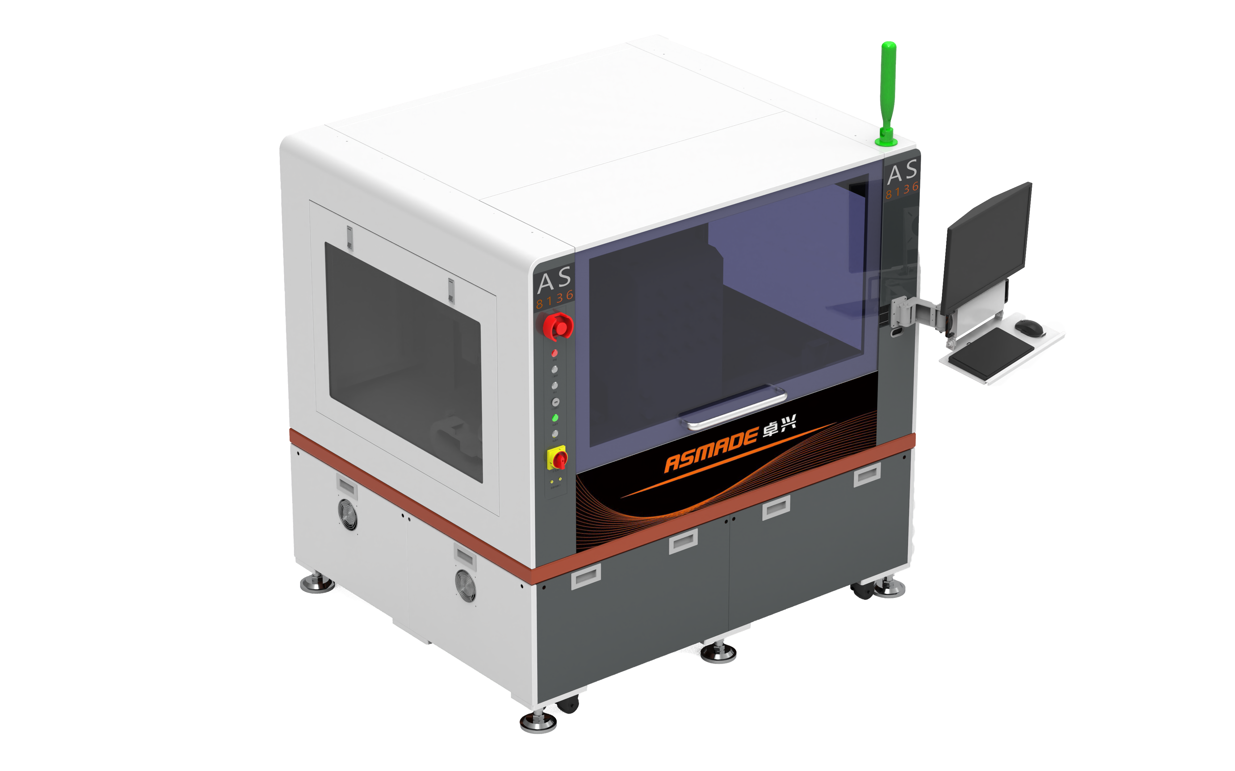
As electronic manufacturing evolves toward miniaturization and high performance, chip packaging processes face increasing challenges in precision, efficiency, and quality. Zhuoxing Semiconductor's AS7301 chip-level printer, with its industry-unique on-chip printing technology and core advantages of precise positioning and efficient printing, has become a key piece of equipment in high-end electronic manufacturing scenarios.On-chip printing technology overcomes quality and efficiency issues in power device dispensing, achieving high-precision mass production.Building on mature technological foundations, and to further meet industry production demands, the AS7301 chip-level printer has added three core new features, achieving a technological breakthrough and completing a comprehensive upgrade in production flexibility, stability, and intelligence. This provides robust support for enterprises to reduce costs and increase efficiency, contributing to the high-quality development of the electronic manufacturing industry.These three core configurations—the compatible magazine and stack feeder assembly, automatic solder paste addition function, and optional AOI component—are innovative solutions developed by Zhuoxing Semiconductor specifically targeting pain points in power device packaging production. The configuration upgrades cover the entire production process of "feeding - solder paste addition - quality inspection," achieving dual optimization of production workflow and product quality through flexible adaptation, intelligent operation, and precise control. Their application scope covers mainstream power device packaging scenarios such as high-power diodes, MOS tubes, DrMOS, and multi-chip Clip.Dual-Mode Flexible Feeding: Breaking Single Limitations, Adapting to Diverse ProductionTraditional feeding equipment has single functions, only suitable for either stack or magazine feeding methods, making it difficult to accommodate both small-batch, multi-specification and large-volume, standardized production needs. This forces enterprises to purchase additional dedicated equipment, increasing costs and space occupancy. Moreover, production changeovers involve complex debugging, frequently affecting continuous production line operation.The AS7301's new dual-mode flexible feeding system adopts a modular design, achieving "one machine, dual modes." By quickly replacing components, it can flexibly adapt to multi-specification production tasks without requiring additional equipment purchases, thereby reducing costs and increasing efficiency.Stack Feeding: Suitable for high-volume continuous production, improving stack material handling efficiency.Magazine Feeding: Adapts to standardized magazines, facilitating material management and changeovers.Customers can switch freely based on order requirements, achieving seamless transition from R&D small batches to large-scale production, greatly enhancing production line responsiveness and equipment utilization.Intelligent Automatic Solder Paste Addition: Precise Quantity Control, Eliminating Manual RelianceThe solder paste process is critical for determining soldering quality. Traditional manual addition methods have inherent limitations, including high variability in addition precision, susceptibility of solder paste to oxidation, and volatility of flux. The newly introduced automatic solder paste addition system on the AS7301 achieves precision and stability upgrades in the process through intelligent closed-loop control.Precise Metering: Automatically executes based on parameters, ensuring consistency in the amount of solder paste added.Dynamic Controllability: Continuously supplies small amounts of solder paste, reducing its exposure time to air.Quality Assurance: Inhibits oxidation and moisture absorption, maintains flux activity, ensuring reliable soldering.Cost Optimization: Precisely controls usage, reducing waste and saving costs.Fully Automatic: Realizes unmanned solder paste addition, improving overall efficiency.AOI Component: Real-Time Inspection, Data-Driven, Closed-Loop Quality ControlTraditional printing quality relies on manual spot checks, which suffer from low efficiency, susceptibility to missed inspections, and lack of systematic data support. Printing quality determines the success or failure of subsequent processes. The newly integrated AOI component in the AS7301 enables full-process control, enhancing quality assurance levels and reducing quality risks.Precise Identification: Online real-time detection of glue dot area, position offset, and shape integrity.Immediate Interception: Alarms immediately upon detecting anomalies, allowing rapid intervention to block defective products from flowing out.Data Closed Loop: Automatically records defect information and generates reports, supporting integration with MES systems.Process Optimization: Based on long-term data accumulation, reversely optimizes printing parameters, continuously improving first-pass yield.The AS7301 chip-level printer, centered on the industry-exclusive on-chip printing technology, deeply integrates the advantages of high-precision narrow-edge printing for fitting, closed-loop pressure control for uniform glue dots, and stepless steel mesh adjustment for efficient production. By superimposing the three upgraded configurations of dual-mode flexible feeding, intelligent automatic solder paste addition, and AOI real-time inspection, it builds a comprehensive competitive advantage of "core technology + full-process optimization." With its ±0.01mm position accuracy, ±0.025mm angle accuracy, and capability to adapt to complex processes like 3D step printing, it comprehensively covers precision packaging scenarios for power devices such as high-power diodes, MOS tubes, and multi-chip Clip. It precisely meets the technical demands of miniaturization and high integration in high-end electronic manufacturing, as well as the complex packaging requirements for high-density interconnection of multiple chips. Simultaneously, its stable performance solidifies the quality foundation, simplifies production lines, lowers the operational threshold, providing an efficient and reliable integrated printing solution for productions of all scales.About UsFounded by an internationally leading team of motion control experts and bringing together the industry's top packaging technology specialists, we are a national high-tech enterprise and a specialized and sophisticated "Little Giant" enterprise with over 20 years of technological accumulation and market practice, focusing on the R&D, manufacturing, and sales of high-precision semiconductor equipment.Our main products include semiconductor packaging equipment, power device packaging equipment, Mini LED chip transfer equipment, intelligent control equipment, and semiconductor packaging process management systems.We are committed to providing customers with one-stop overall solutions for semiconductor packaging processes. Our products feature fully independent intellectual property rights, and many of our equipment models are industry firsts.
March 19, 2026
Learn More
Total 6 items
1
2
Go to
Page
Booth activities
Contact Us
ASMADE Semiconductor Technology Limited
深圳市卓兴半导体科技有限公司
深圳市卓兴半导体科技有限公司
Explore more of our services
Our Booth No.
E5
.
5272
5272
Please read carefully
Disclaimer
Join our social media
©Messe Muenchen Shanghai Co., Ltd.
 沪公网安备31011502016746号