Exhibitor Profile
Suzhou Jutai HPM Co., Ltd.
苏州聚泰新材料有限公司
苏州聚泰新材料有限公司
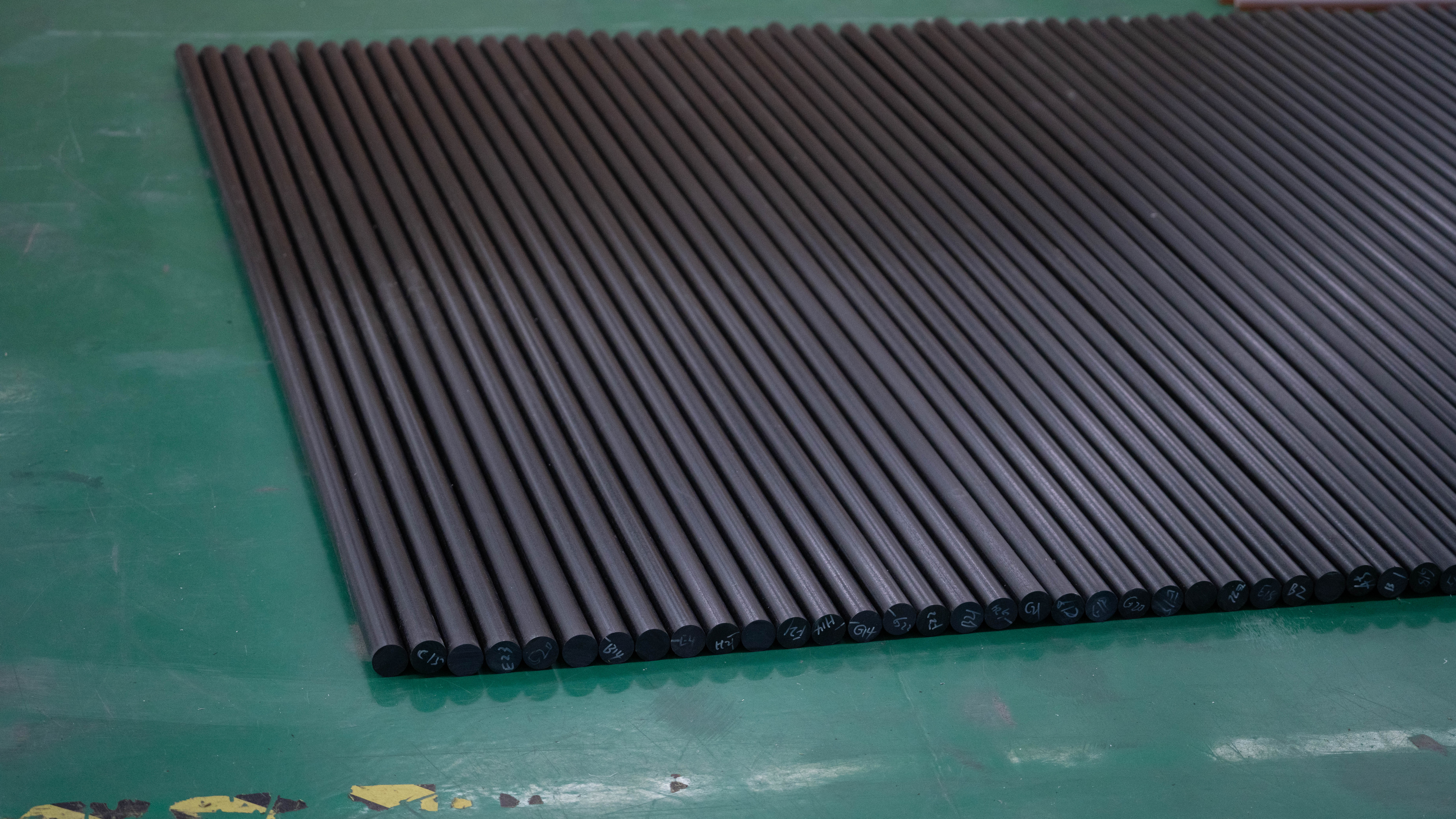
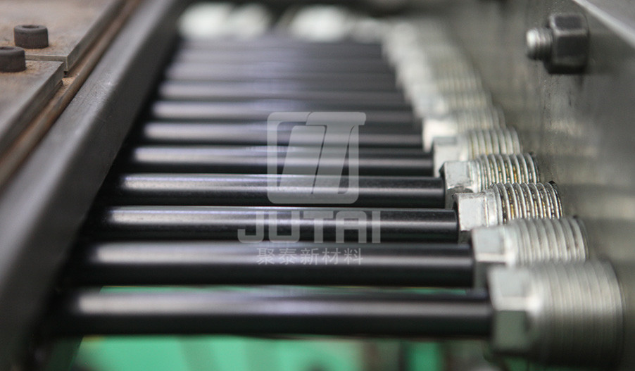
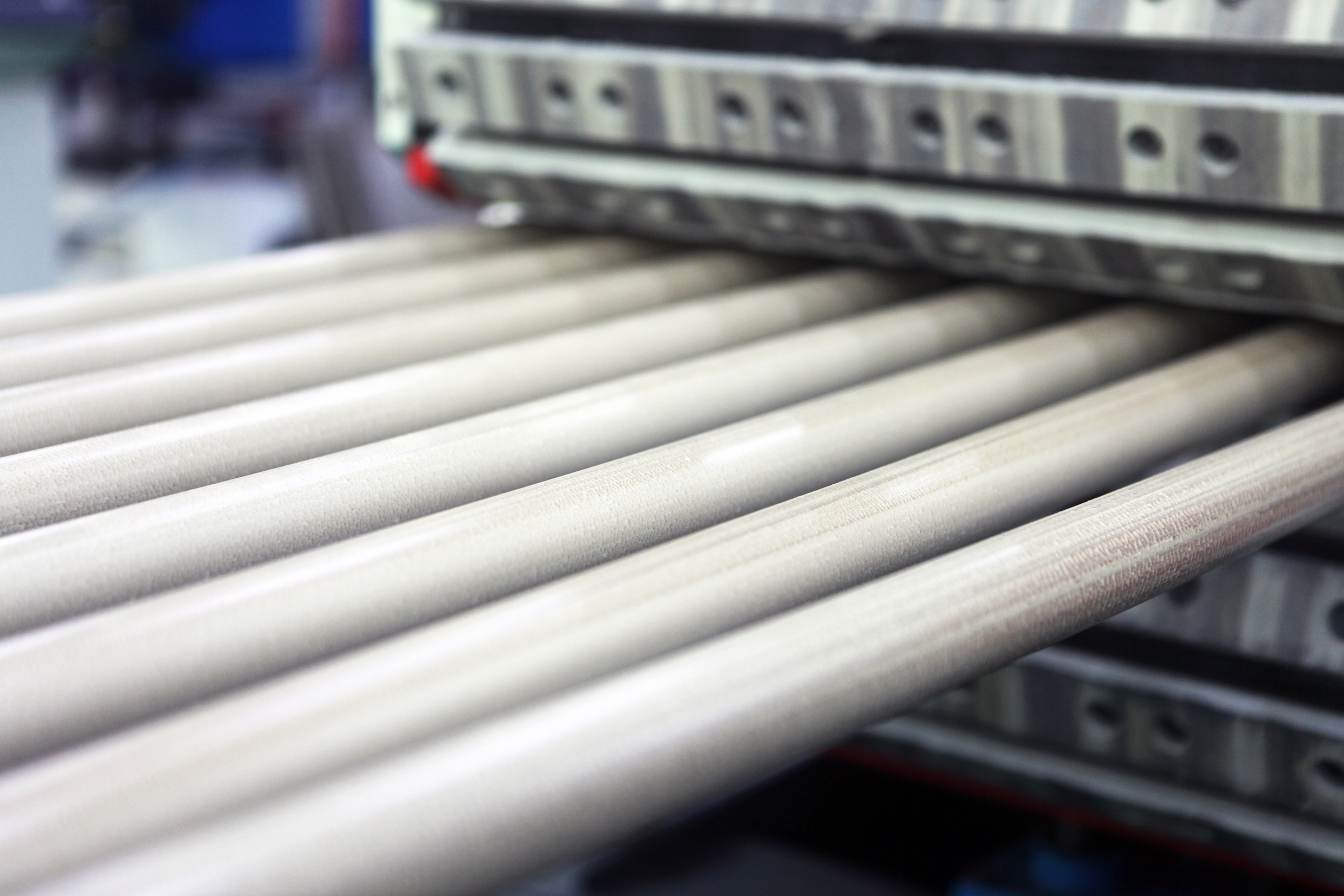
Suzhou Jutai New Materials Co., Ltd. specializes in providing integrated solutions for special engineering plastics to clients across various industries. Leveraging its full industry chain advantages—from raw material selection and custom compound formulation to product structure design optimization and assembly—the company delivers personalized solutions from raw materials to finished products for end-users. It has multiple established product series, including PAEK (Polyaryletherketone), PEI (Polyetherimide), PSU (Polysulfone), PI (Polyimide), and PPS (Polyphenylene Sulfide).
Booth No.:
W2.2928
Country:
Product Category:
Electronic Chemical Materials
Production technologies for cable processing and connectors
Robotics, AGV
Industrial sensor
Automated Electronics Assembly
Application Area:
Industrial Electronics
Communication Systems
Consumer Electronics
Household appliances
Automotive Industry
Medical Technology
New Energy
Aviation&Space Technology
Military Electronics
Mechanical Engineering
Rail Transit
Product Information
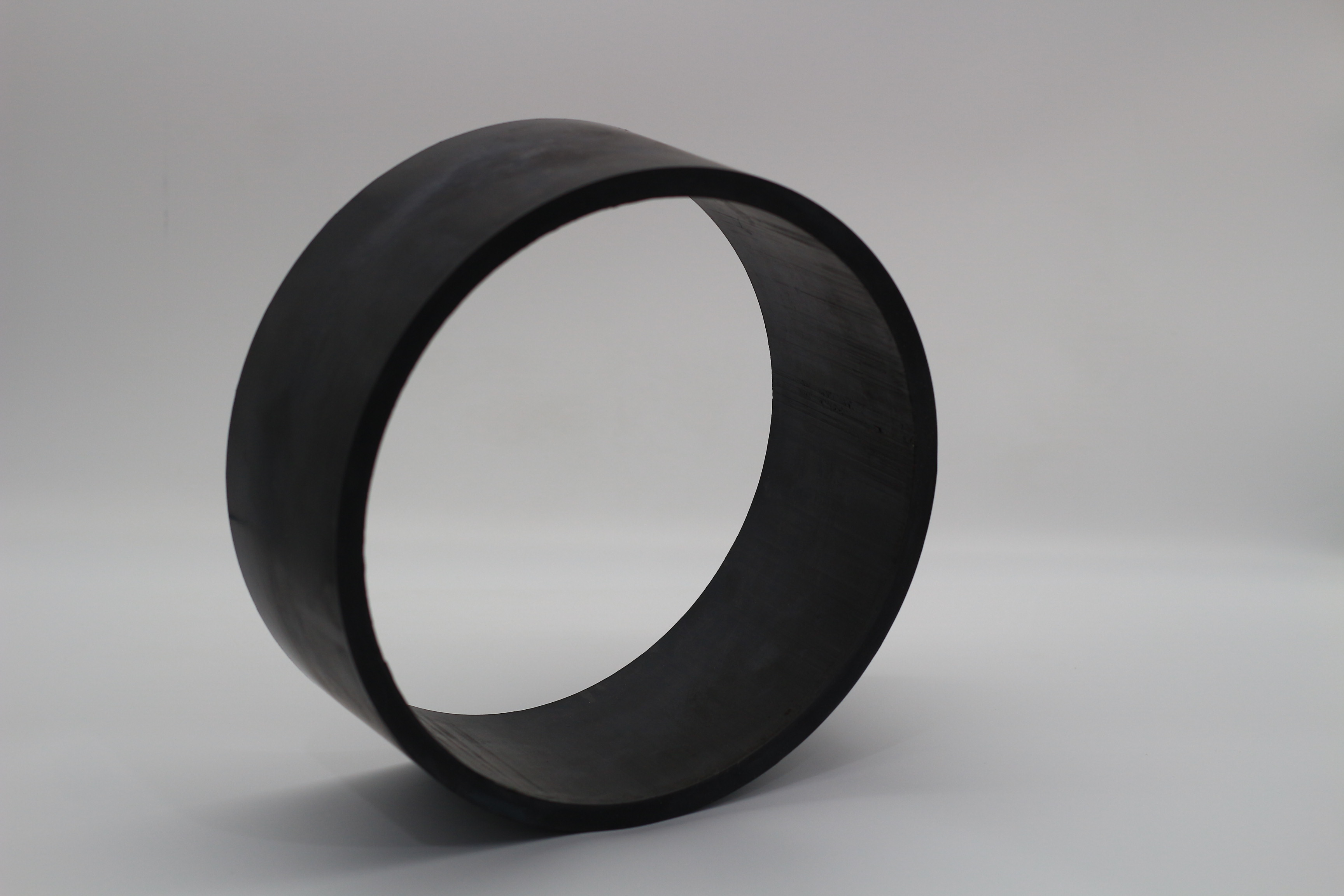
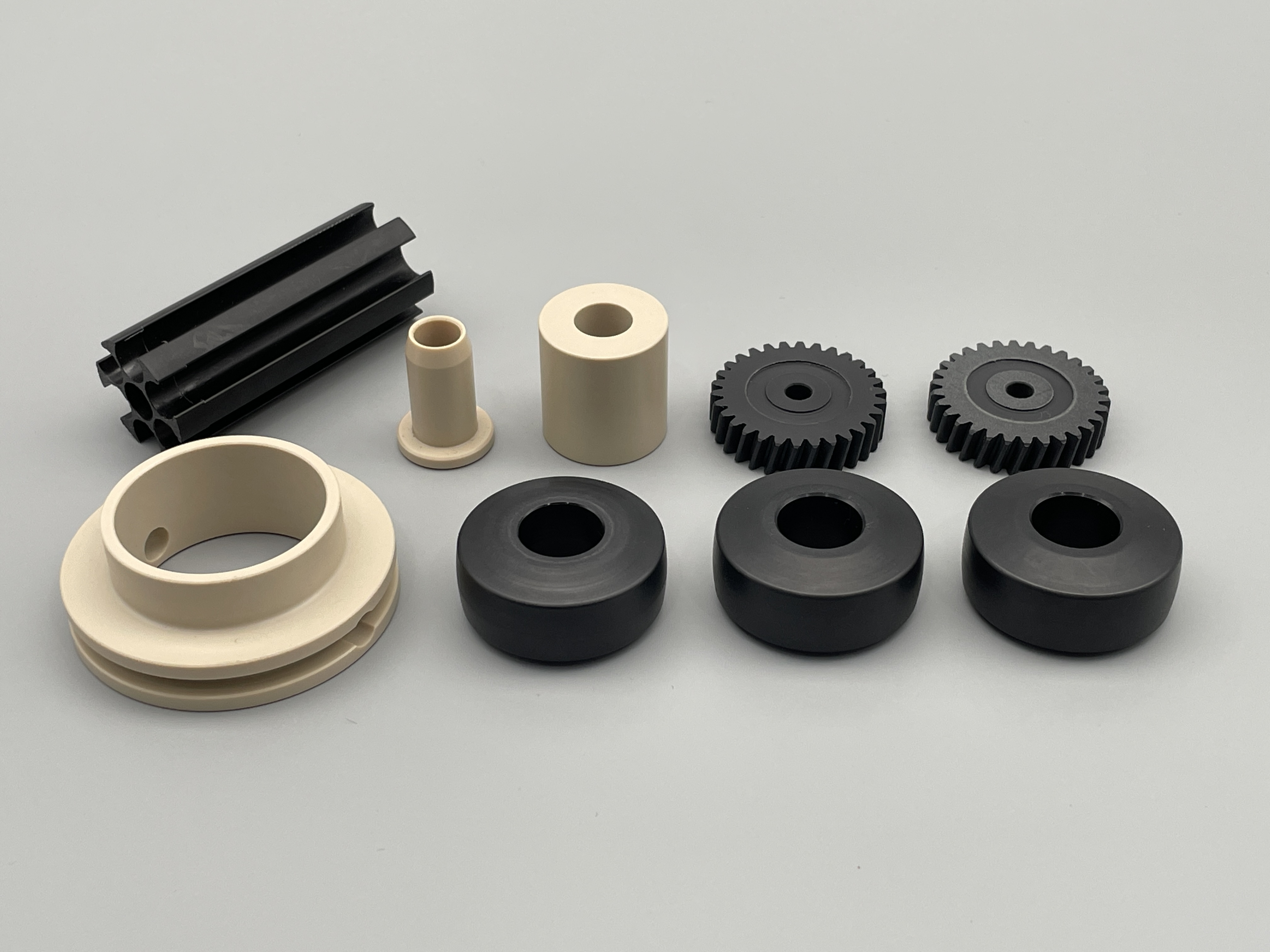
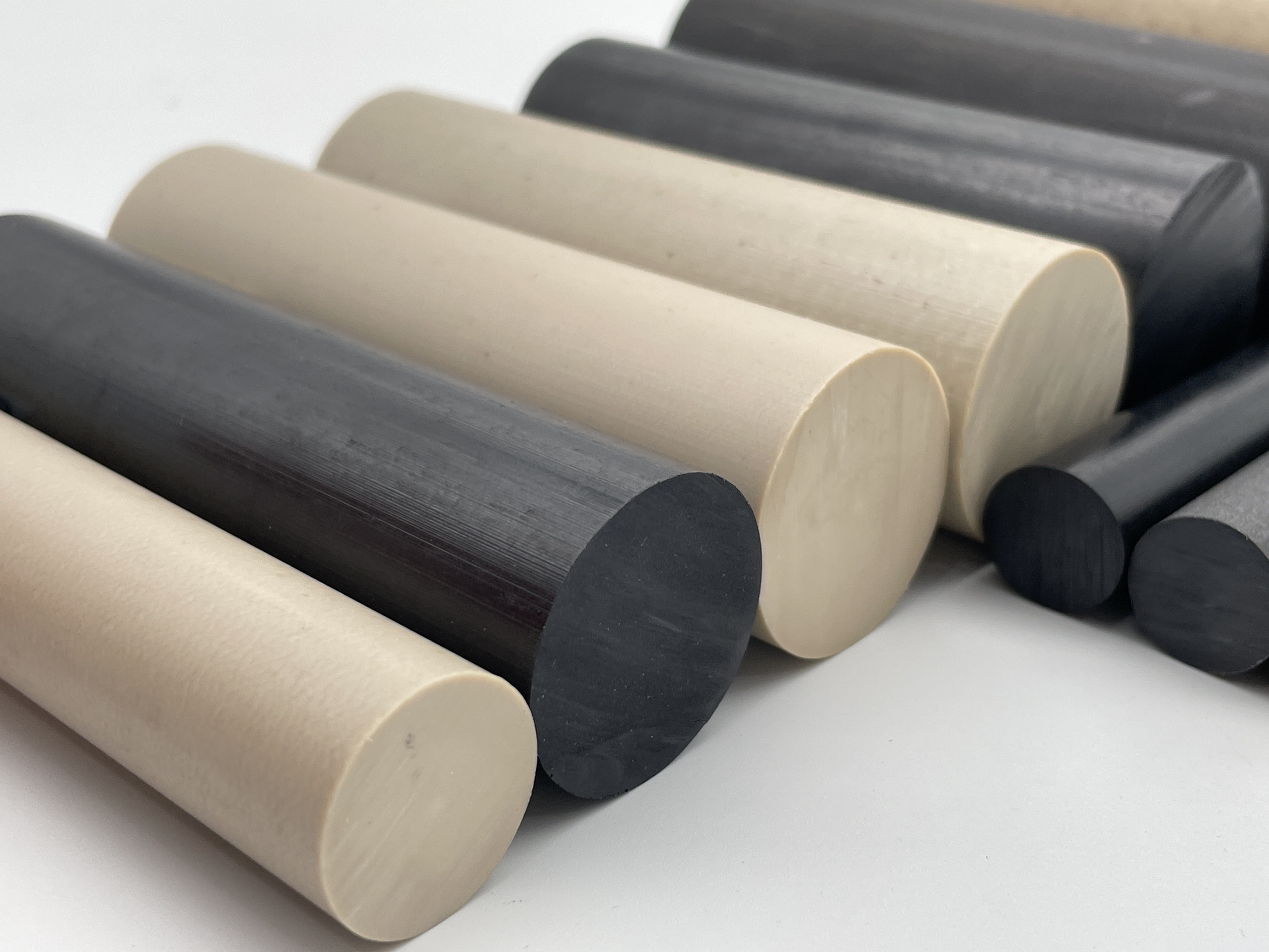
Conventional Products
Product Category:
Electronic Chemical Materials
Application Area:
Conventional Products
Product Category:
Electronic Chemical Materials
Application Area:
Product Category:
Electronic Chemical Materials
Application Area:
A total of 7 items
1
2
Go to
Page
Exhibitor News
News Title
News Contents
Publication Time
10¹⁰–10¹² Ω: The “Critical Threshold” of Antistatic PEEK — How to Balance Performance and Safety?
March 3, 2026
In semiconductor fabrication environments, static electricity is invisible and intangible — yet its destructive power is measured in nanoseconds.Direct breakdown:The human body typically cannot sense electrostatic discharge (ESD) below 3,000 V. However, for chips with line widths of only a few nanometers, an accidental discharge of just a few dozen volts can puncture the gate oxide layer, rendering an entire wafer scrap.Potential Induced Damage (PID):Even more concerning is low-voltage discharge. The chip may not fail immediately, but internal “hidden damage” remains, leading to early product failure and becoming a reliability time bomb.Particle attraction:Charged surfaces act like vacuum cleaners, attracting microscopic airborne particles. In a Class 10 cleanroom, a single 0.1 μm particle landing in a photolithography area can destroy the entire wafer pattern.Therefore, from wafer fabrication to packaging, testing, and transportation, antistatic materials are essential. However, different processes and contact conditions require different levels of static control — which brings us to the question of resistivity selection.The Antistatic Material Family: Four Resistivity Ranges, Four “Roles”The core parameter of antistatic materials is surface resistivity (unit: Ω). It is not “the lower, the better,” but rather “the better the match, the better the performance.” These four categories can be understood as four different “roles” in a semiconductor facility.10¹⁰–10¹² Ω Antistatic PEEK: Engineered for “Critical Scenarios”In semiconductor manufacturing, certain applications impose seemingly contradictory requirements:The material must prevent static, yet remain electrically insulating; withstand high temperatures, yet maintain cleanliness; retain the mechanical strength of PEEK, while providing antistatic functionality.This is precisely where 10¹⁰–10¹² Ω antistatic PEEK finds its purpose. It does not replace conductive or dissipative materials — instead, it fills the “gap” between insulation and conductivity.1. Suppressing Charge Generation — Not Relying on GroundingThe core logic of dissipative materials (10⁶–10⁹ Ω) is “rapid discharge,” which requires a reliable grounding path. However, in certain precision structures, grounding may be impractical or may interfere with electrical design.Materials in the 10¹⁰–10¹² Ω range follow a different approach:Charge suppression: Material modification reduces the likelihood of triboelectric charge generation.Slow neutralization: If charges are generated, they dissipate gradually through micro-conduction pathways or neutralize via ambient ions.Applicable scenarios: Ideal for applications where grounding is inconvenient, or where both electrical insulation and antistatic performance are required.2. Preserving PEEK’s “Flagship Properties” Without CompromiseConductive PEEK (<10⁵ Ω) typically requires high carbon filler loading. While conductivity improves, mechanical properties may decline (e.g., increased brittleness).In contrast, 10¹⁰–10¹² Ω antistatic PEEK achieves static control through intrinsic or low-additive technologies, preserving PEEK’s inherent strengths, including:High temperature resistance (continuous use up to 260 °C)Excellent mechanical strength (capable of replacing metal in certain applications)Chemical resistance (withstands strong acids and alkalis during cleaning processes)Low ionic extractables (protecting wafer purity)3. Bridging the Gap Between “Insulative” and “Dissipative”Standard PEEK (Insulator >10¹² Ω): Suitable for high-insulation requirements, but may accumulate static under high-speed friction.Dissipative materials (10⁶–10⁹ Ω): Suitable for grounded applications requiring rapid discharge.Antistatic PEEK (10¹⁰–10¹² Ω): Positioned in between — capable of gradually releasing static to prevent accumulation while maintaining insulating properties and not interfering with circuit design.It is not “better,” but “different” — providing a professional solution for applications that require PEEK performance, antistatic functionality, and electrical insulation simultaneously.Typical Engineering Applications of JUTAIPEEK® ESD 10#12Semiconductor IC test socketsWafer handling components (waffle pads, trays)Probe station componentsInsulating structural supportsJUTAI’s Next-Generation Antistatic TechnologyProduct Property Table:
March 3, 2026
Learn more
Booth Activities
Contact Us
Suzhou Jutai HPM Co., Ltd.
苏州聚泰新材料有限公司
苏州聚泰新材料有限公司
Explore our additional services

Our Booth No.
W2
.
2928
2928
Please read carefully.
Disclaimer
Join our social media
©Messe Muenchen Shanghai Co., Ltd.
 沪公网安备31011502016746号